
- English
- Español
- Português
- русский
- Français
- 日本語
- Deutsch
- tiếng Việt
- Italiano
- Nederlands
- ภาษาไทย
- Polski
- 한국어
- Svenska
- magyar
- Malay
- বাংলা ভাষার
- Dansk
- Suomi
- हिन्दी
- Pilipino
- Türkçe
- Gaeilge
- العربية
- Indonesia
- Norsk
- تمل
- český
- ελληνικά
- український
- Javanese
- فارسی
- தமிழ்
- తెలుగు
- नेपाली
- Burmese
- български
- ລາວ
- Latine
- Қазақша
- Euskal
- Azərbaycan
- Slovenský jazyk
- Македонски
- Lietuvos
- Eesti Keel
- Română
- Slovenski
- मराठी
- Srpski језик

Home
>
Products > Signal Jammer Module > Anti Drone Signal Jammer Module > Ultra-Wideband C-Band 4-8 GHz 50W Power Amplifier RF System


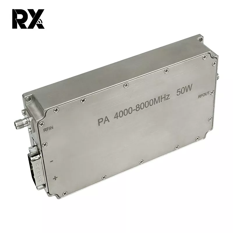
Ultra-Wideband C-Band 4-8 GHz 50W Power Amplifier RF System
This 50W broadband power amplifier is a high-performance RF module designed for applications requiring robust output power across the 4 GHz to 8 GHz frequency range. Utilizing advanced GaN (Gallium Nitride) technology, it delivers high power density, excellent efficiency, and reliable linearity over a wide instantaneous bandwidth. The amplifier is engineered for stability, durability, and consistent performance in demanding environments.
Send Inquiry
Product Description
Key Features
Broadband Performance: Operates seamlessly across the full 4 GHz to 8 GHz (C-Band) spectrum without the need for band switching.
High Output Power: Delivers a typical saturated output power of 50 Watts (47 dBm) minimum across the band.
High Gain: Features a typical small-signal gain of 50 dB (minimum), ensuring effective signal amplification from low-power sources.
Excellent Gain Flatness: Maintains superior gain flatness of typically ±1.5 dB over the entire frequency range for uniform performance.
High Efficiency: Incorporates high-efficiency design, typically achieving 30% Power Added Efficiency (PAE), reducing thermal load and DC power consumption.
Robust Linear Performance: Offers high 1 dB compression point (OP1dB) typically > 47 dBm, supporting both linear and saturated amplification for various modulation schemes.
Integrated Protection & Control: Includes comprehensive safety features: Reverse Voltage Protection, Over-Temperature Shutdown, and Output Overload / VSWR Protection. Standard analog interface for bias control, enable/disable (TTL), and status monitoring.
Thermal Management: Designed with an efficient baseplate cooling system to ensure reliable operation under full load conditions. Operational case temperature range: -40°C to +85°C.
Ruggedized Construction: Housed in a robust, hermetically sealed metal package for superior shielding and environmental resilience, suitable for military, aerospace, and industrial applications.
|
No. |
Description |
Symbol |
Min |
Typ |
Max |
Unit |
Remark |
|
1. |
Operating Frequency |
BW |
4000 |
|
8000 |
MHz |
|
|
2. |
Input Power |
Pin |
|
0 |
|
dBm |
|
|
3. |
Output Power CW |
Psat |
47 |
48.5 |
49.5 |
dBm |
Continuous Wave |
|
4. |
Power Gain |
Gp |
47 |
|
49.5 |
dBm |
@ Pin=0 dBm |
|
5. |
Power Gain Flatness |
△Gp |
|
±1.5 |
|
dB |
@ Pin=0 dBm |
|
6. |
Small SignalGain |
G |
49 |
50.5 |
52 |
dB |
@ Pin=-5dBm |
|
7. |
Small SignalGain Flatness |
△G |
|
±2 |
|
dB |
@ Pin=-5dBm |
|
8. |
Input Return Loss |
S11 |
|
-15 |
|
dB |
|
|
9. |
Operating Voltage |
Vdc |
28 |
28 |
32 |
V |
|
|
10. |
Current Consumption |
A |
|
6 |
8 |
A |
@ Pout=50~90W |
|
11. |
Working Temperature |
|
-40℃~+50℃ |
|
|
||
|
12. |
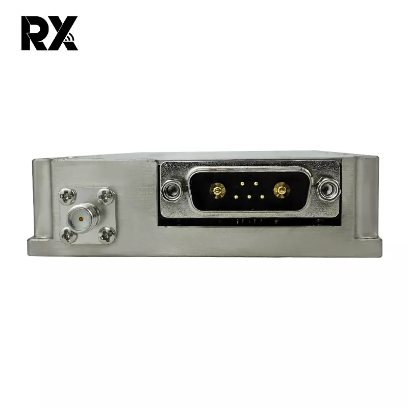
RF Connector Input |
|
SMA, Female |
|
|
||
|
13. |
RF Connector Output |
|
SMA, Female |
|
|
||
|
14. |
Weight |
|
|
0.439 |
0.50 |
Kg |
|
|
15. |
Length*Width*Height |
|
134*80*22 |
mm |
|
||
|
16. |
Input Power |
PinMax |
-5 |
|
5 |
dBm |
|
|
17. |
Interface Definition (7W2 Female) |
VDD |
A1 |
Ground |
|
||
|
GND |
A2 |
28Vdc |
|
||||
|
Current Sense |
1 |
Analog voltage relative to Module’s current@100mV/A |
|
||||
|
Temp Sense |
2 |
Analog voltage relative to Module’sTemperature@10mV/℃ |
|
||||
|
Enable |
3 |
Amplifier Enable |
Amplifier Enable:TTL Logic High(3.3V) (Internally Pulled-Low) |
||||
|
GND |
4 |
Ground |
|
||||
|
|
Overall dimension |
Note:
1、 The overall dimensions are for reference only; 2、 The size can be appropriately increased or decreased according to the customer's requirements; 3、 The positions of the input interface, output interface and power supply interface can be changed according to the actual needs of the customers; |
|||||

Hot Tags: Ultra-Wideband C-Band 4-8 GHz 50W Power Amplifier RF System, China, Manufacturers, Suppliers, Wholesale, Factory, Customized, Brands, Quality, 1 Years Warranty
Related Category
Send Inquiry
Please feel free to give your inquiry in the form below. We will reply you in 24 hours.


